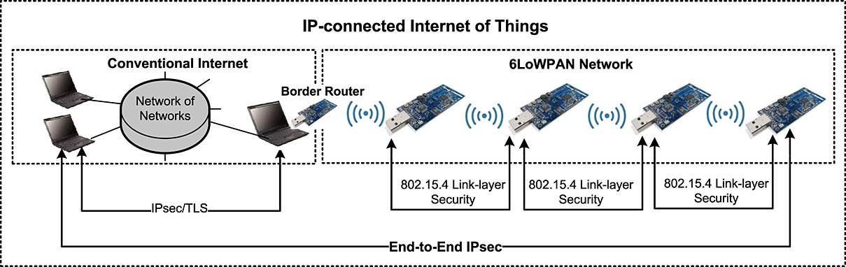
Designing optimum LED drivers for Industrial, commercial and consumer applications requires a clear understanding of the application requirements. To achieve power factor correction, low total-harmonic-distortion (THD) and good output current control while meeting increasing cost and efficiency targets, only the most appropriate switching topology will suffice. Since there is no standardization in LED load voltage requirements, no single “best topology “exists.
The aim of this month’s article is to explore off-line conversion and examine the factors that determine where buck, buck-boost, tapped-buck and flyback topologies are most effective.
Highest efficiency and lowest cost, input voltage range, output voltage range, THD, PF, regulatory requirements and the cost of isolated versus non-isolated topologies are all factors that need to be considered in selecting the appropriate driver.
Available Topologies
The simplest switching conversion approach is to use a buck converter – it has the lowest component count, a very simple (low cost) magnetic component (an inductor) and the highest efficiency. The use of single stage combined PFC and CC controllers means that for PFC and low ATHD, buck converters are an attractive choice for non-isolated designs.
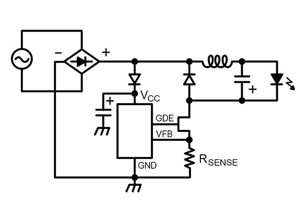
Figure 1. High-Side Buck Circuit using a Combined PFC and CC Output Integrated Control + Switching IC (Note that a high value aluminum electrolytic bulk capacitor is not required) [3]
Buck converters cannot provide functional isolation and requires the input voltage to be higher than the output voltage to work. The latter issue is important when considering THD. It can be shown that in order to meet EN61000-3-2 C/D standards for THD, the output voltage from a low-line input buck converter must be less than approximately 35 VDC. This limit is needed to keep the conduction angle (the proportion of the switching cycle over which the switching circuit is able to conduct and therefore influence input current wave-shape) high enough to effectively shape the input current to meet THD limits. For high-line applications, the maximum output voltage is approximately 70 to 75 V. In addition, Buck converters are not good at controlling voltage step-down if the ratio of input to output voltage is greater than approximately 8:1 due to duty cycle limitations in the controller.
Buck-Boost Converter
Buck-boost conversion is the next alternative – component count is similar to buck designs and efficiency is also very high. Buck-boost converters operate across a wider portion of the available conduction angle and so can provide good THD for higher output voltage designs. They have a similar problem with isolation and duty cycle limited input/output voltage ratio as buck converters.
Figure 2. Non-Isolated Buck-Boost Converter Employing Combined PFC and CC Single Stage Converter IC
Tapped-Buck Converters
The next category to consider as a possible solution is tapped-buck converters. The more complex winding structure of the magnetic element introduces a cost and efficiency penalty. However the transformer/inductor nature of the winding structure allows a turns-ratio type adjustment of output voltage and current, making tapped buck converters good for standard designs where the input to output ratio precludes the use of a buck or buck-boost topology. It is appropriate to consider the tapped buck converter as analogous to a non-isolated flyback converter
Figure 3. A low Power Tapped-Buck Converter (With no PFC stage)
Note the Wide-Input Voltage Range
Flyback Converters
The final category of LED driver we will consider is the flyback converter. The converter can be implemented as either isolated or non-isolated and the turns-ratio capability of the transformer allows for pretty much any ratio of input to output voltage. Due to imperfect coupling between primary and secondary windings, as well as primary parasitic capacitance, the more complex winding arrangement leads to increased cost and power losses. Flyback converters are overwhelmingly used for isolated LED bulb designs and use either a passive-valley fill PFC circuit (Valley fill is acceptable for 0.7 PF applications but induce 8 to 10 percent efficiency penalty in reaching the 0.9 PF required for commercial applications), or higher-efficiency combined CC and PFC converters that are available today.
Figure 4. High Efficiency Combined PFC and CC Converter in an Isolated Flyback Topology
Choosing the Right Topology
A summary of the decision process to select between different topologies is shown below. The selection strategy assumes the following order for designs: Buck →Buck Boost →Tapped Buck → Flyback. The order is weighted; highest efficiency and lowest cost being the most desirable requirements.
Figure 5. Topology Selection Flow Chart
Only if the best topology for each design is selected, can performance be guaranteed and the best design delivered. Every design will be different but all can follow the methodology described in this paper for deriving the most ideal solution for each application type.