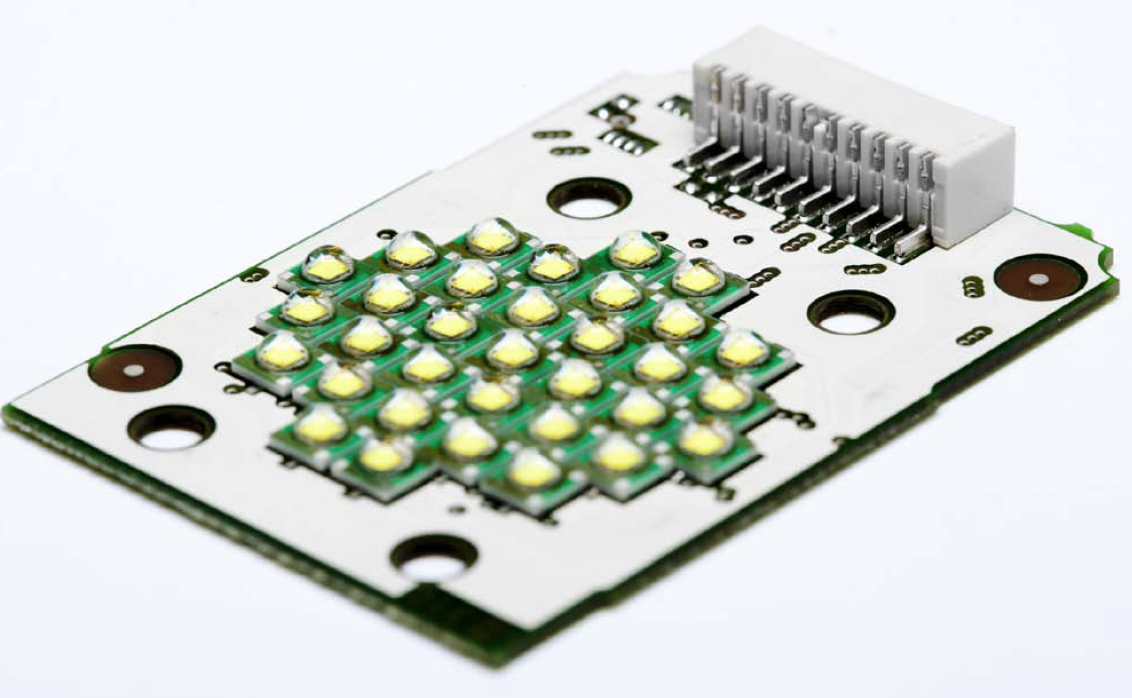
Despite the enormous efficiency advantages of LEDs, when compared to incandescent lights, they still waste around 70 percent of the electrical energy put into them. This energy appears as heat and needs to be conducted away from the LED to maintain a safe operating temperature. Overheating an LED severely limits its lifespan and impacts on efficiency and color quality.
Existing thermal management technologies are limiting the speed at which LEDs can penetrate into certain high-powered application areas. They simply cannot deliver the technical performance required at acceptable cost. Huge opportunities therefore exist for companies that can find a more cost-effective substrate solutions for high brightness LEDs.
Conventional Approaches
The key characteristics required for a thermal substrate are excellent thermal conductivity and good electrical isolation. This limits the materials choice. Aluminum nitride (AIN) has traditionally been used in high brightness chip on board (COB) LEDs and as a submount for high power LEDs.
Whilst aluminum nitride is thermally more than up to the job the exotic manufacturing process – requiring carbonthermal reduction of aluminum oxide or direct nitridation of aluminum, together with the extremely high temperatures involved – makes it very expensive. Currently available machinery limits the size that can be manufactured to around 4 inches by 4 inches. It is also quite brittle, which in turn limits the yield. Add to this the requirement for specialist processors and you end up with a very uneconomical product.
The use of aluminum itself is a very compelling option – it’s a great thermal conductor, cheap, readily available and extremely robust. What it lacks is electrical isolation. The standard approach of adding an epoxy to the surface to produce a dielectric layer reduces the thermal conductivity too much for use with high brightness LEDs so an alternative is needed.
Attempts to anodize the surface of aluminum to combine the thermal conductivity of aluminum with the dielectric properties of a ceramic have failed repeatedly over the years – the anodizing process leaves gaps in the dielectric layer, which can create electrical short circuits.
A New Approach:
Cambridge Nanotherm has taken a new approach, patenting an entirely original electrochemical process for creating a dielectric on the surface of aluminum. This process produces a composite substrate with thermal properties comparable to AlN but far more cost effective.
Nanotherm’s approach converts the surface of a sheet of aluminum into a dielectric nanoceramic layer. The crystals formed can be as small as 30 to 60 nanometers. Because the nanoceramic is formed by a conversion process, this ensures a perfect and robust bond between the dielectric and the aluminum resulting in a uniform layer of ceramic, which is a perfect dielectric.
The nanoceramic dielectric layer can be as thin as 3 microns, this makes the thermal path between the LED chip and the aluminum as small as is feasibly possible, resulting in extremely high overall thermal conductivity.
What’s more the nanoceramic layer can be grown just as easily on complex 3D shapes. This is key to the creation of vias. With AIN, creating vias is expensive, complex and creates mechanical weakness. With the Nanotherm process, holes can simply be drilled in the aluminum before processing and the ceramic dielectric will be deposited uniformly on the surface of these through-holes.
The Result:
The resulting nanoceramic dielectric layer has a thermal conductivity of around 7.2 W/mK and a dielectric measure of about 50 V/um. For COB LEDs, the finished product has a thermal conductivity of 152 W/mK (measured between the top surface of the copper that carries the wiring trace and a 0.6 mm aluminum sheet). This outperforms many low-grade and mid-grade AIN products. Double-sided metallization, with through-holes yields sub-mounts for LEDs.
Cost is always a factor. With an industry in desperate need of finding ways to bring the cost of LED products down to a point that the mass market are comfortable with, any saving is good. Not only do nanoceramic substrates offer a significant cost advantage over AIN, they can also be processed through standard PCB manufacturing facilities, bringing the scale and cost advantages of the traditional PCB industry to bear on the LED packaging market for the first time.
Nanoceramics open up an entirely new class of thermal management aimed squarely at the high power LED market.


